1 大连理工大学光电工程与仪器科学学院,辽宁 大连 116024
2 中国科学院理化技术研究所,北京 100190
3 中国科学院微电子研究所,北京 100029
对基于行波电极的硅-有机复合集成电光调制器进行研究,构建调制器的波导电极结构模型,分析特征阻抗和微波有效折射率对调制器频率响应的影响。通过对电极结构的仿真优化,完成调制器芯片的设计与制备,研究电光聚合物材料的片上极化工艺,得到高性能硅-有机复合集成电光调制器。对研制调制器电极的电学S(Scatter)参数进行测试,分析得到的电极特征阻抗和有效折射率与仿真设计结果基本相符。测试得到电光调制器的3 dB带宽大于50 GHz。
集成光学 电光调制器 硅-有机复合集成 行波电极 3 dB带宽 光学学报
2023, 43(23): 2313002

Author Affiliations
Abstract
School of Optoelectronic Engineering and Instrumentation Science, Dalian University of Technology, Dalian 116024, China
In-band full-duplex (IBFD) technology can double the spectrum utilization efficiency for wireless communications, and increase the data transmission rate of B5G and 6G networks and satellite communications. RF self-interference is the major challenge for the application of IBFD technology, which must be resolved. Compared with the conventional electronic method, the photonic self-interference cancellation (PSIC) technique has the advantages of wide bandwidth, high amplitude and time delay tuning precision, and immunity to electromagnetic interference. Integrating the PSIC system on chip can effectively reduce the size, weight, and power consumption and meet the application requirement, especially for mobile terminals and small satellite payloads. In this paper, the silicon integrated PSIC chip is presented first and demonstrated for IBFD communication. The integrated PSIC chip comprises function units including phase modulation, time delay and amplitude tuning, sideband filtering, and photodetection, which complete the matching conditions for RF self-interference cancellation. Over the wide frequency range of C, X, Ku, and K bands, from 5 GHz to 25 GHz, a cancellation depth of more than 20 dB is achieved with the narrowest bandwidth of 140 MHz. A maximum bandwidth of 630 MHz is obtained at a center frequency of 10 GHz. The full-duplex communication experiment at Ku-band by using the PSIC chip is carried out. Cancellation depths of 24.9 dB and 26.6 dB are measured for a bandwidth of 100 MHz at central frequencies of 12.4 GHz and 14.2 GHz, respectively, and the signal of interest (SOI) with 16-quadrature amplitude modulation is recovered successfully. The factors affecting the cancellation depth and maximum interference to the SOI ratio are investigated in detail. The performances of the integrated PSIC system including link gain, noise figure, receiving sensitivity, and spurious free dynamic range are characterized.
Photonics Research
2023, 11(10): 1635

Author Affiliations
Abstract
1 University of Southern Denmark, Center for Nano Optics, Odense, Denmark
2 Kiel University, Institute for Experimental and Applied Physics, Kiel, Germany
3 University of Stuttgart, Research Center SCoPE, 4th Physics Institute, Stuttgart, Germany
Electrically connected optical metasurfaces with high efficiencies are crucial for developing spatiotemporal metadevices with ultrahigh spatial and ultrafast temporal resolutions. While efficient metal–insulator–metal (MIM) metasurfaces containing discretized meta-atoms require additional electrodes, Babinet-inspired slot-antenna-based plasmonic metasurfaces suffer from low efficiencies and limited phase coverage for copolarized optical fields. Capitalizing on the concepts of conventional MIM and slot-antenna metasurfaces, we design and experimentally demonstrate a new type of optical reflective metasurfaces consisting of mirror-coupled slot antennas (MCSAs). By tuning the dimensions of rectangular-shaped nanoapertures atop a dielectric-coated gold mirror, we achieve efficient phase modulation within a sufficiently large range of 320 deg and realize functional phase-gradient metadevices for beam steering and beam splitting in the near-infrared range. The fabricated samples show (22 % ± 2 % ) diffraction efficiency for beam steering and (17 % ± 1 % ) for beam splitting at the wavelength of 790 nm. The considered MCSA configuration, dispensing with auxiliary electrodes, offers an alternative and promising platform for electrically controlled reflective spatiotemporal metasurfaces.
optical reflective metasurfaces beam steering beam splitting Advanced Photonics Nexus
2023, 2(1): 016005

Author Affiliations
Abstract
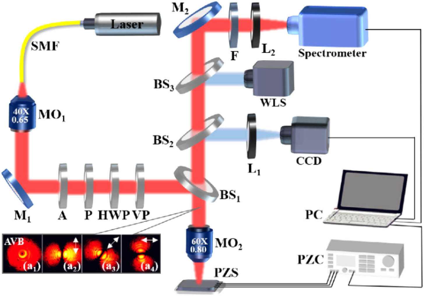
Key Laboratory of Light Field Manipulation and Information Acquisition, Ministry of Industry and Information Technology, and Shaanxi Key Laboratory of Optical Information Technology, School of Physical Science and Technology, Northwestern Polytechnical University, Xi’an 710129, China
Noble metallic nanostructures with strong electric near-field enhancement can significantly improve nanoscale light–matter interactions and are critical for high-sensitivity surface-enhanced Raman spectroscopy (SERS). Here, we use an azimuthal vector beam (AVB) to illuminate the plasmonic tips circular cluster (PTCC) array to enhance the electric near-field intensity of the PTCC array, and then use it to improve SERS sensitivity. The PTCC array was prepared based on the self-assembled and inductive coupled plasmon (ICP) etching methods. The calculation results show that, compared with the linearly polarized beam (LPB) and radial vector beam excitations, the AVB excitation can obtain stronger electric near-field enhancement due to the strong resonant responses formed in the nanogap between adjacent plasmonic tips. Subsequently, our experimental results proved that AVB excitation increased SERS sensitivity to 10-13 mol/L, which is two orders of magnitude higher than that of LPB excitation. Meanwhile, the PTCC array had excellent uniformity with the Raman enhancement factor calculated to be . This kind of vector light field enhancing Raman spectroscopy may be applied in the field of sensing technologies, such as the trace amount detection.
surface-enhanced Raman spectroscopy plasmonic tips circular cluster array azimuthal vector beam surface plasmon polaritons Chinese Optics Letters
2023, 21(3): 033603

Author Affiliations
Abstract
1 MOE Key Laboratory of Material Physics and Chemistry under Extraordinary Conditions and Shaanxi Key Laboratory of Optical Information Technology, School of Physics Science and Technology, Northwestern Polytechnical University, Xi’an 710072, China
2 MOE Key Laboratory of Weak-Light Nonlinear Photonics, TEDA Applied Physics Institute and School of Physics, Nankai University, Tianjin 300457, China
We present the generation of the nanosecond cylindrical vector beams (CVBs) in a two-mode fiber (TMF) and its applications of stimulated Raman scattering. The nanosecond (1064 nm, 10 ns, 10 Hz) CVBs have been directly produced with mode conversion efficiency of ~18 dB (98.4%) via an acoustically induced fiber grating, and then the stimulated Raman scattering signal is generated based on the transmission of the nanosecond CVBs in a 100-m-long TMF. The transverse mode intensity and polarization distributions of the first-order Stokes shift component (1116.8 nm) are consistent with the nanosecond CVBs pump pulse.
vector beam stimulated Raman scattering fiber grating Chinese Optics Letters
2021, 19(1): 010603
中国农业大学现代精细农业系统集成研究教育部重点实验室, 北京 100083
农田变量施肥作业需要对农田土壤养分信息进行高精度的快速原位采集, 已有的设备不能满足精细农业田间测量的需要, 为此基于近红外漫反射测量开发了一款新型车载式原位土壤参数检测仪。 检测仪采用光照稳定性更好的卤钨光源代替太阳光进行土壤光谱检测, 以提高仪器对工作条件的适应性。 由7个敏感波长(1 070, 1 130, 1 245, 1 375, 1 450, 1 550, 1 680 nm)构成的土壤氮素测量极限学习机模型提高了仪器的测量实时性和精度。 检测仪由机械部分、 光学部分及控制部分组成。 机械部分为检测仪提供平台支撑, 光学部分为检测仪提供检测光源, 主要由卤钨光源、 光源转接法兰、 近红外导光光纤、 检测总成(含入射光出口端、 InGaAS光电探测器及7个敏感波长的滤光片)等组成, 控制部分实现对土壤测量信号的采集及处理。 检测仪工作时, 卤钨光源通过近红外导光光纤、 检测总成中的入射光出口端将检测光源传输到待测土壤表面, 通过测量土壤表面漫反射光的光谱反射率检测土壤养分参数。 在卤钨光源和近红外导光光纤连接处设计光源转接法兰, 最大限度的减小检测光源在传输过程中的损失。 漫反射光经过检测总成中的滤光片滤波后, 由相应的InGaAS光电探测器实现光电转换, 再经信号处理单元计算出各个敏感波长处的反射率。 检测仪采用灰度标准板进行光学标定测试, 测试结果显示, 检测仪在7个敏感波长处的反射率与MATRIX-I型傅里叶光谱分析仪反射率相关系数最高为0.997 8, 平均值为0.927 8, 表明检测仪有较高的检测精度。 为进一步对检测仪农田土壤养分的检测精度进行评估, 进行了检测仪的农田应用试验, 检测结果表明检测仪检测值与实验室标准检测方法检测值的相关系数都在0.90以上。 试验结果表明, 车载式原位土壤参数检测仪能够实现对农田土壤养分信息的快速原位高精度检测。
近红外光谱学 漫反射 土壤养分 车载式原位检测仪 Near infrared spectroscopy Diffuse reflection Soil nutrients Vehicle-mounted in-situ detector 光谱学与光谱分析
2020, 40(9): 2856
吕衍秋 1,2,3,*彭震宇 1,2,3曹先存 1,2,3何英杰 1,3[ ... ]朱旭波 1,2,3
1 中国空空导弹研究院, 河南 洛阳 471099
2 红外探测器技术航空科技重点实验室, 河南 洛阳 471099
3 河南省锑化物红外探测器工程技术研究中心, 河南 洛阳 471099
InAs/GaSb超晶格材料制备的新型红外器件在最近十几年得到了迅速发展。文中开展了InAs/GaSb二类超晶格中/短波双色焦平面探测器组件研制, 设计了中/短波双色叠层背靠背二极管芯片结构, 用分子束外延技术生长出结构完整、表面平整、低缺陷密度的PNP结构超晶格材料, 制备出性能优良的320×256双色焦平面探测器组件, 对探测器组件进行了测试分析。结果显示, 在77 K下中波二极管RA值达到26.0 kΩ·cm2, 短波的RA值为562 kΩ·cm2。光谱响应特性表明短波响应波段为1.7~3 μm, 中波为3~5 μm, 满足设计要求。双色峰值探测率达到中波3.12×1011 cm·Hz1/2W-1, 短波1.34×1011 cm·Hz1/2W-1。响应非均匀性中波为9.9%, 短波为9.7%。中波有效像元率为98.46%, 短波为98.06%。
InAs/GaSb超晶格 双色 中短波 焦平面阵列 红外探测器 InAs/GaSb superlattice dual-color mid-/short-wavelength FPAs infrared detector 红外与激光工程
2020, 49(1): 0103007
Author Affiliations
Abstract
1 MOE Key Laboratory of Material Physics and Chemistry under Extraordinary Conditions and Shaanxi Key Laboratory of Optical Information Technology, School of Science, Northwestern Polytechnical University, Xi’an 710072, China
2 e-mail: ting.mei@ieee.org
Surface-enhanced Raman spectroscopy (SERS) with high-sensitivity performance is a very necessary detection technology. Here, we present a method for increasing the performance of SERS based on silver triangular nanoprism arrays (ATNAs) vertically excited via a focused azimuthal vector beam (AVB). The ATNA substrates with different structural parameters are prepared based on the traditional self-assembled and modified film lift-off technique. Based on a theoretical model established adopting the structural parameters of the ATNA substrates, theoretical simulation results show that AVB excitation can achieve greater electric-field enhancement than linearly polarized beam (LPB) excitation. Experimental result indicates that SERS sensitivity obtained via AVB excitation is (1 M = 1 mol/L) using rhodamine 6G (R6G) as the target analyte, which is 2 orders of magnitude lower than that of LPB excitation (). Meanwhile, the uniformity and reproducibility of the ATNA substrates are examined using Raman mapping and batch-to-batch measurement, respectively, and the Raman enhancement factor is calculated to be . This method of vector light field excitation may be used to improve the SERS performance of the substrates in fields of ultra-sensitive Raman detection.
Photonics Research
2019, 7(12): 12001447
1 中国空空导弹研究院,河南 洛阳 471099
2 驻中国空空导弹研究院军事代表室,河南 洛阳 471099
3 红外探测器技术航空科技重点实验室,河南 洛阳 471099
4 河南科技大学电子信息工程学院,河南 洛阳 471003
制冷型InSb红外焦平面探测器工作时需降温至低温(80 K),器件在整个生命周期会经受从常温(300 K)到低温(80 K)的上千次高低温循环。针对该型探测器开展了高低温循环特性试验,测试和分析了上千次高低温循环过程中器件光电性能、杜瓦热负载和J-T制冷器特性的变化。试验结果表明,探测器可以经受至少2 000次高低温循环,并且探测率变化的幅度≤5.5%、响应率变化的幅度≤4.8%、盲元数未发生增加。研究结果为器件的工艺研发和改进提供了参考。
InSb焦平面探测器 高低温循环 参数变化 可靠性 InSb infrared focal plane array detectors thermal cycle parameter variation reliability 红外与激光工程
2015, 44(12): 3701
1 海军驻洛阳地区航空军事代表室, 河南 洛阳 471009
2 中国空空导弹研究院红外探测器技术航空科技重点实验室, 河南 洛阳 471009
激光成像制导是精确制导的主要发展方向之一。激光成像制导探测器是激光成像 系统的关键部件。介绍了国内外激光成像制导探测器的研究进展,包括HgCdTe焦平面、Si雪崩焦平 面、InGaAs PIN探测器和雪崩光电二极管(Avalanche Photodiode, APD)焦 平面。InGaAs APD焦平面将会成为激光成像制导探测器的主要发展方向,其 关键技术包括外延材料生长、高均匀性探测器制备以及读出电路设计等。
激光成像制导 探测器 焦平面 雪崩光电二极管 laser imaging guidance detector FPA APD


